


Intel Advances Progress in Integrated Photonics for Data Centers
What’s New: At Intel Labs Day, Intel highlighted industry-leading technology advances toward realizing the company’s long-standing vision of integrating photonics with low-cost, high-volume silicon. The advancements represent critical progress in the field of optical interconnects, which address growing challenges around the performance scaling of electrical input/output (I/O) as compute-hungry data workloads increasingly overwhelm network traffic in data centers. Intel demonstrated advances in key technology building blocks, including miniaturization, paving the way for tighter integration of optical and silicon technologies.
“We are approaching an I/O power wall and an I/O bandwidth gap that will dramatically hinder performance scaling. Intel’s rapid progress in integrated photonics will enable the industry to fully re-imagine data center networks and architectures that are connected by light. We have now demonstrated all of the critical optical technology building blocks on one silicon platform, tightly integrated with CMOS silicon. Our research on tightly integrating photonics with CMOS silicon can systematically eliminate barriers across cost, power, and size constraints to bring the transformative power of optical interconnects to server packages.”
Why it matters: New data-centric workloads are growing every day within the data center, with ever-increasing data movement from server to server that is taxing the capabilities of today’s network infrastructure. The industry is quickly approaching the practical limits of electrical I/O performance. As bandwidth demand for computing keeps increasing, electrical I/O isn’t scaling to keep pace, resulting in an “I/O power wall” that limits available power for computing operations. By bringing optical I/O directly into our servers and onto our packages, we can break down this barrier, enabling data to move more efficiently.
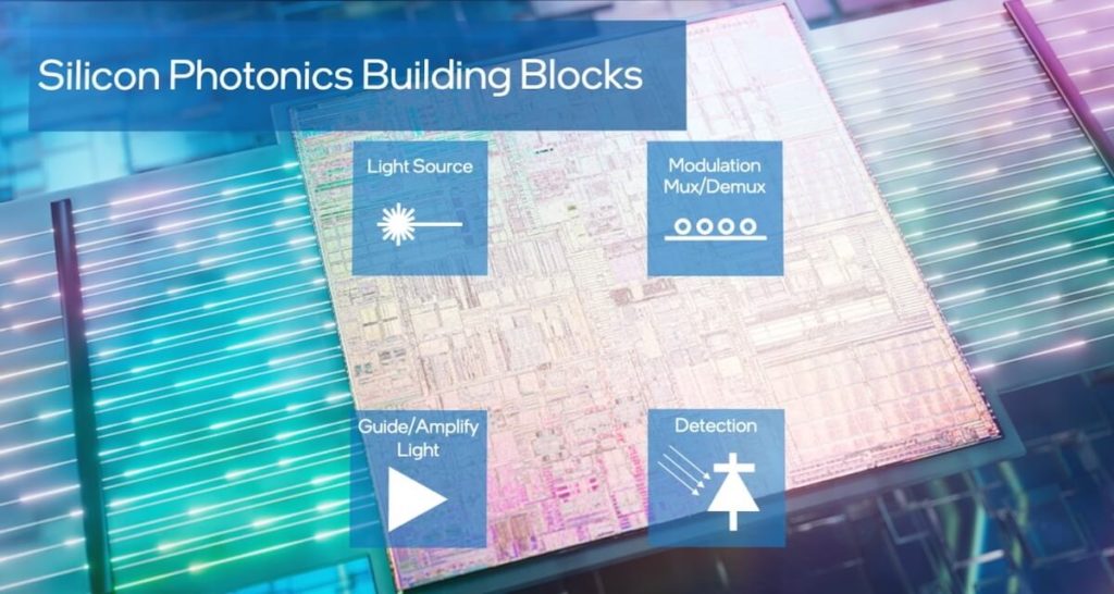
New Technology Building Blocks: At the Intel Labs virtual event, Intel demonstrated the key to progress in critical technology building blocks that are fundamental to its integrated photonics research. These technology building blocks, including light generation, amplification, detection, modulation, complementary metal-oxide-semiconductor (CMOS) interface circuits, and package integration, are essential to achieve integrated photonics. A prototype shown at the event featured tight coupling of photonics and CMOS technologies, serving as a proof-of-concept of future full integration of optical photonics with core compute silicon. Intel also showcased micro-ring modulators that are 1000x smaller than traditional components. The large size and cost of conventional silicon modulators have been a barrier to bringing optical technology onto server packages, which require the integration of 100s of these devices. These combined results pave the way for the extended use of silicon photonics beyond the network’s upper layers to inside the server and onto future server packages.
Key technology building blocks showcased:
- Micro-ring modulators: Conventional silicon modulators take up too much area and are costly to place on IC packages. By developing micro-ring modulators, Intel has miniaturized the modulator by a factor of more than 1000, thereby eliminating a key barrier to integrating silicon photonics onto a computing package.
- All-silicon photodetector: For decades, the industry has believed silicon has virtually no light detection capability. Intel showcased research that proves otherwise. Lower cost is one of the main benefits of this breakthrough.
- Integrated semiconductor optical amplifier: As we focus on reducing total power consumption, integrated semiconductor optical amplifiers are an indispensable technology, made possible with the same material used for the integrated laser.
- Integrated multi-wavelength lasers: Using a technique called wavelength division multiplexing, separate wavelengths can be used from the same laser to convey more data in the same beam of light. This enables additional data to be transmitted over a single fiber, increasing bandwidth density.
- Integration: By tightly integrating silicon photonics and CMOS silicon through advanced packaging techniques, we can gain three benefits: (1) lower power, (2) higher bandwidth, and (3) reduced pin count. Intel is the only company that has demonstrated integrated multi-wavelength lasers and semiconductor optical amplifiers, all-silicon photodetectors, and micro-ring modulators on a single technology platform tightly integrated with CMOS silicon. This research breakthrough paves the path for scaling integrated photonics.
What’s Next: Integrated photonics research, demonstrated at the event, showcased meaningful progress toward Intel’s ambitious goal initiated many years ago to tap light based on connectivity technology. The new research opens many possibilities, including future architectures that are more disaggregated. Multiple functional blocks such as compute, memory, accelerators, and peripherals spread throughout the entire network and interconnected via optical and software in high-speed and low-latency links.